About
Hammad M. Cheema, et al., "A low‐power 802.11 ad compatible 60‐GHz phase‐locked loop in 65‐nm CMOS" Microwave and Optical Technology Letters 57 (3), 2015, 660.
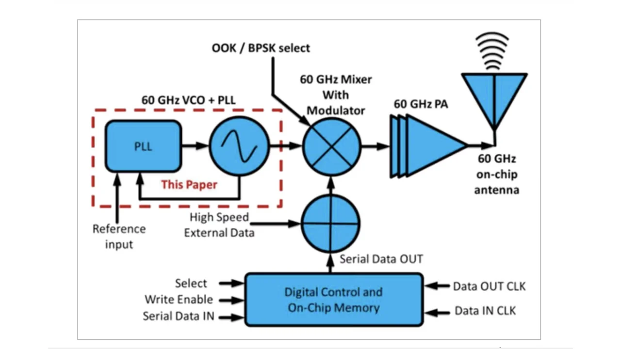
A 60‐GHz fundamental frequency phase locked loop (PLL) as part of a highly integrated system‐on‐chip transmitter with on‐chip memory and antenna is presented. As a result of localized optimization approach for each component, the PLL core components only consume 30.2 mW from a 1.2 V supply. A systematic design procedure to achieve high phase margin and wide locking range is presented. The reduction of parasitic and fixed capacitance contributions in the voltage controlled oscillator enables the coverage of the complete 802.11 ad frequency band from 57.2 to 65.8 GHz. A new 4‐stage distribution network supplying the local oscillator (LO) signal to the mixer, the feedback loop and the external equipment is introduced. The prescaler based on the static frequency division approach is enhanced using shunt‐peaking and asymmetric capacitive loading. The current mode logic based divider chain is optimized for low power and minimum silicon foot‐print. A dead‐zone free phase frequency detector, low leakage charge pump, and an integrated second‐order passive filter completes the feedback loop. The PLL implemented in 65 nm CMOS process occupies only 0.6 mm2 of chip space and has a measured locking range from 56.8 to 66.5 GHz. The reference spurs are lower than −40 dBc and the in‐band and out‐of‐band phase noise is −88.12 dBc/Hz and −117 dBc/Hz, respectively. © 2015 Wiley Periodicals, Inc. Microwave Opt Technol Lett 57:660–667, 2015
